
Physics of Nanostructures
Nanostructure properties connect geometry and interfaces to quantum states, carrier occupation, and electrical, optical, or magnetic response. The governing scales are confinement energy, thermal energy, mean free path, coherence length, and interaction strength.
1. Nanoscale structure and physical regimes
1.1 Dimensionality and characteristic lengths
A nanostructure typically has at least one dimension of about 1-100 nm; 1 nm equals 10 Å. Its physical regime depends on how its size compares with the carrier wavelength, exciton radius, mean free path, and coherence length. A metal particle and a semiconductor dot of equal size need not exhibit equally strong quantum confinement.
Electronic dimensionality counts the directions of free motion. A quantum well confines one direction and supports a 2D electron system. A quantum wire confines two directions and is 1D. A quantum dot confines all three and is 0D. Multiple occupied transverse subbands must be included even in a geometrically thin structure.
Confinement changes allowed energies and the density of states. Coherence allows amplitudes along different paths to interfere. Surfaces and interfaces alter bonding, strain, defects, and charge distributions. Mesoscopic behavior combines microscopic quantum effects with macroscopic statistical behavior; it is not defined by a universal size interval.
1.2 Surface fraction, metastability, and device scaling
For a sphere of radius R, the surface-to-volume ratio is 3/R. A surface shell of thickness t occupies the stated fraction, with the approximation valid for t much smaller than R. At R = 5 nm and t = 0.3 nm, the shell occupies about 17% of the volume. Coordination, adsorbates, reconstruction, and ligands therefore strongly affect properties.
Top-down fabrication uses lithography, etching, and machining to define structures. Bottom-up fabrication builds them through molecular chemistry, nucleation, and growth. Positioning and interconnection often favor top-down methods; composition and atomic structure can favor bottom-up growth. Nanostructures frequently occupy metastable free-energy minima and may transform during annealing or environmental changes.
A MOSFET controls a source-drain channel electrostatically. Thinner gate dielectrics increase gate tunneling, while shorter channels enhance source-drain tunneling and drain-induced barrier lowering. Gates surrounding the channel improve electrostatic control, but tunneling, contacts, interconnect RC delay, and heat removal remain relevant. Smaller dimensions alone do not guarantee lower total power or faster systems.
1.3 Conditions for observing quantum effects
Transport is ballistic when L is much smaller than the mean free path and usually diffusive when L is much larger. Coherence is a separate comparison with Lφ; a diffusive sample can remain coherent. Static elastic scattering can preserve coherence, while environmental coupling, dynamic defects, or spin flips can dephase carriers. The square-root length expressions apply to diffusion; ballistic propagation uses velocity times time.
Resolved levels require their spacing to exceed thermal and lifetime or disorder broadening. Thermal energies are about 25.85 meV at 300 K and 0.345 meV at 4 K. A 1 meV feature is generally thermally smeared at room temperature. Fermi wavelength, exciton Bohr radius, and magnetic length diagnose different confinement mechanisms.
Screening length measures the range over which carriers suppress a perturbing potential. In the 3D Thomas-Fermi approximation, q_TF²=e²D₃D(E_F)/(ε₀ε_r), with screening length 1/q_TF. This assumes slowly varying potentials and local response; 2D screening requires a different treatment.
A metal grain has mean level spacing δ≈1/[D₃D(E_F)V]. When it approaches the superconducting gap, the bulk continuum pairing picture becomes inadequate and superconducting signatures are suppressed or modified. This criterion differs from comparing grain size with superconducting coherence length; electron-number parity can also matter.
2. Quantum mechanics in reduced dimensions
2.1 Wavefunctions, Hamiltonians, and boundary conditions
The squared wavefunction gives probability density. A stationary state has a time-independent density, whereas a superposition can evolve. A plane wave has definite momentum but is spatially delocalized; a localized particle requires a wave packet. Plane waves on infinite space are not square-normalizable, so finite-box normalization or delta normalization is used.
The constants satisfy ℏ = h/(2π); kinetic-energy expressions written in terms of wavevector use ℏ. Across a finite nonsingular potential with equal masses, the wavefunction and its derivative are continuous. An infinite hard wall imposes ψ = 0. For a position-dependent effective mass, the Hermitian divergence-form kinetic operator leads to continuity of ψ and the normal mass-weighted derivative.
Electromagnetic fields couple through scalar and vector potentials. For an electron q = -e, with e positive. Canonical and mechanical momentum differ in a magnetic field. Specify the energy reference, charge sign, boundary conditions, and mass before solving a confinement problem.
2.2 The infinite square well
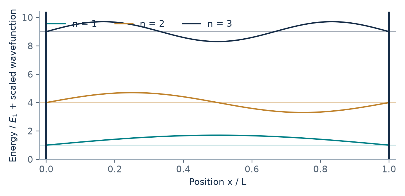
Inside 0<x<L, the solution is a combination of sine and cosine. The left boundary eliminates cosine and the right imposes kL=nπ. Normalization fixes the amplitude. The n=0 solution vanishes identically and is not a state. The ground state has no internal nodes; state n has n-1 nodes and increasing level spacing.
Halving the confinement width quadruples the energies, and a smaller effective mass increases them. For m*=0.067m₀ and L=10 nm, E₁≈56.1 meV and the first spacing is about 168.4 meV. Finite barriers lower these values and limit the bound-state count. The envelope approximation requires variations slow on the lattice scale.
2.3 Finite wells and bound-state counting
For a well of width L with V=-V₀ inside and zero outside, bound energies satisfy -V₀<E<0. Solutions oscillate inside and decay outside. Inversion symmetry separates even cosine solutions from odd sine solutions; both must join normalizable exponential tails.
Solve these transcendental equations graphically or numerically. The first even branch always intersects the decaying-tail condition, giving at least one bound state for every nonzero attractive 1D square well. Its penetration length is 1/κ and grows near the continuum threshold. A threshold state at E=0 is not square-normalizable.
The ceiling formula excludes zero-energy threshold states. Away from integer values it equals floor of the argument plus one; exactly at an integer that alternative overcounts by one. Confinement does not imply complete electrical insulation: quantum-well states conduct in-plane, and contacted dots can conduct by tunneling.
2.4 Subbands in wells, wires, and dots
Separation of variables makes total energy a sum over directions. Each transverse quantum-number set defines a subband edge Eₐ, with continuous dispersion along unconfined directions. A single-subband description requires the chemical potential below the next edge and weak thermal excitation. Dots have discrete spectra, with orbital degeneracies and shells controlled by symmetry.
Closed shells can enhance cluster stability, but magic numbers depend on geometry, interactions, and the confining potential. Finite barriers couple neighboring wells or dots, splitting isolated levels into bonding and antibonding combinations. Periodic arrays can form minibands. Geometry, electronic dimensionality, and coupling strength are distinct descriptors.
2.5 Deriving the density of states
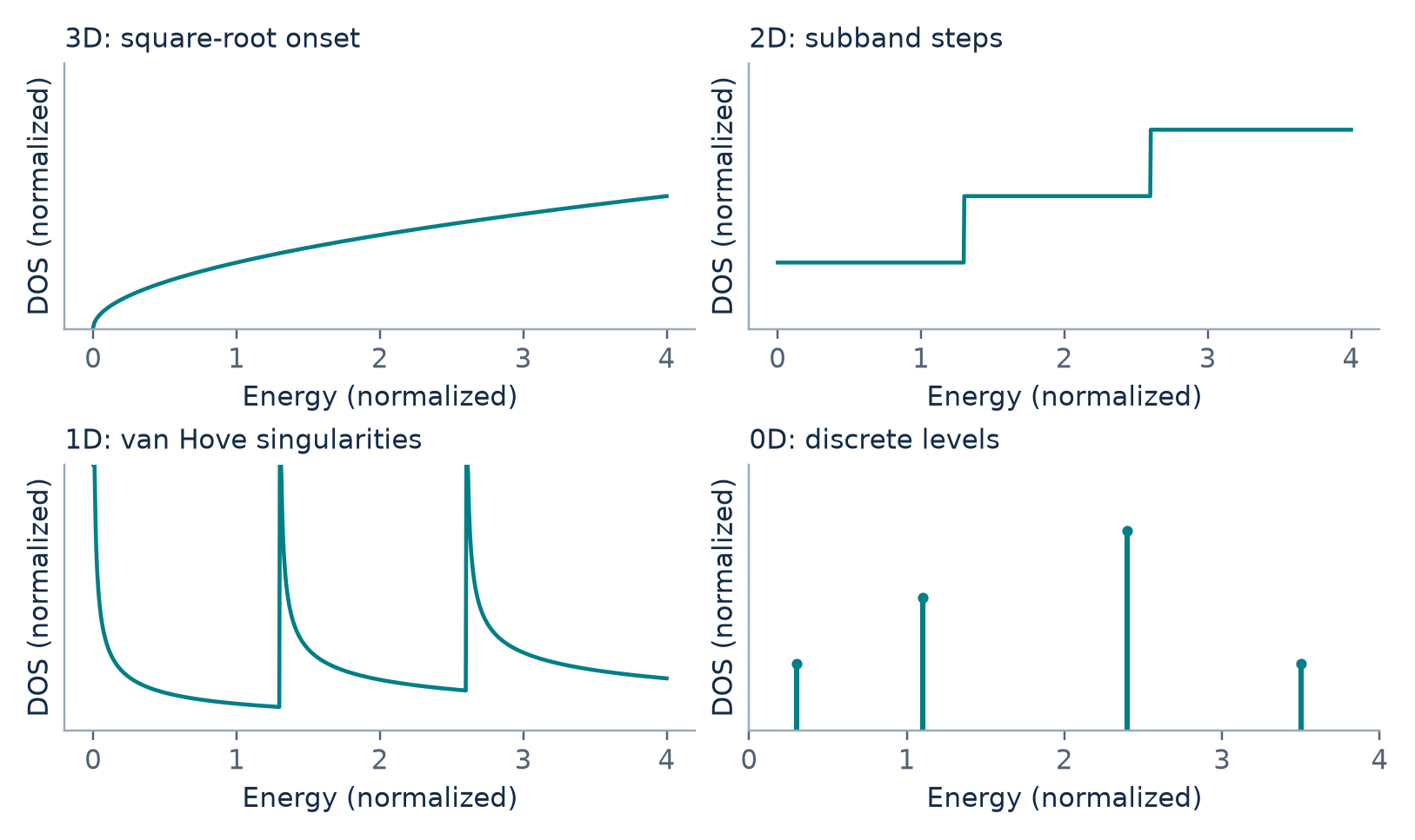
The DOS D(E)dE counts available states, not occupied electrons. Normalize by length in 1D, area in 2D, volume in 3D, and by a single dot in 0D. The following expressions assume spin degeneracy two, a single valley, and an isotropic parabolic band; energies are measured from its edge. Additional valley degeneracy multiplies the result.
Each k state occupies (2π/L)^d. Count an interval of length 2k in 1D, a disk of area πk² in 2D, or a sphere of volume 4πk³/3 in 3D, then multiply by spin degeneracy. Substitute the dispersion and differentiate with respect to energy. Do not count ±k twice when the full interval or shell already includes them.
Sum the 1D expression over wire subbands with their respective thresholds. A 3D parabolic band has a square-root onset, a well has steps, a wire has inverse-square-root van Hove singularities, and a dot has discrete peaks. Temperature, scattering, and instrumental resolution broaden ideal features. Linear-dispersion graphene is an important exception to the parabolic-band scaling.
2.6 Fermi energy and carrier filling
At zero temperature, the Fermi function is a step and electrons fill to E_F. The same expressions follow directly from k-space counting. At finite temperature use the chemical potential μ(T), approximately E_F in the strongly degenerate limit. When several subbands are occupied, solve the number equation using the total DOS.
For n₂=3×10¹¹ cm⁻²=3×10¹⁵ m⁻² and m*=0.067m₀, k_F≈1.37×10⁸ m⁻¹, λ_F≈45.8 nm, and E_F≈10.7 meV. This filling energy is measured above the lowest subband edge, not above the unconfined material band edge.
2.7 Tunneling through barriers
The expression applies to a rectangular barrier of width a for 0<E<V₀, equal masses, and equal potentials on both sides. Match incident and reflected waves, the two barrier exponentials, and the transmitted wave at both interfaces. Transmission is a ratio of probability currents; unequal lead velocities require a velocity factor.
The WKB integral spans the forbidden region between classical turning points and requires a sufficiently slowly varying barrier. For a vacuum electron, its exponential factor is exp[-1.025 a(Å)√(V₀-E)(eV)]. A 1 eV excess barrier over 1 nm gives about 3.54×10⁻⁵ for this factor. Elastic tunneling neither requires thermal activation over the barrier nor an energy loss.
A rough escape rate is an attempt frequency times transmission, ν₀T, giving lifetime 1/(ν₀T). A quasibound state between two barriers can produce resonant tunneling; symmetric coupling can yield nearly unit transmission at resonance even when either barrier alone is weakly transmitting.
2.8 Magnetic confinement and Landau levels
In Landau gauge, orbital motion perpendicular to the field becomes a harmonic oscillator while motion along the field remains free. A true 2DEG has no free k_z contribution. Number levels from n=0. Each Landau level has e|B|/h orbital states per unit area for each spin and valley.
The radius is a semiclassical cyclotron radius inferred from orbital energy, not a definite electron trajectory. The flux quantum is h/e; half-integer orbital flux is distinct from Landau degeneracy. Zeeman splitting is a spin effect, whereas ℏω_c is orbital. Their ratio is |g*|m*/(2m₀) when the parameters are field independent.
3. Solid-state, surface, and optical foundations
3.1 Lattices, reciprocal space, and bands
A crystal combines a Bravais lattice with a basis. Conventional BCC and FCC cells contain two and four lattice points. Diamond is FCC with a two-atom basis of identical atoms; zinc blende uses two species. Three dimensions have seven crystal systems and fourteen Bravais lattices. Miller indices are reduced integer ratios of reciprocal intercepts; [uvw] labels a direction and {hkl} a family of equivalent planes.
Bloch states are plane waves modulated by lattice-periodic functions. Band energies obey Eₙ(k+G)=Eₙ(k), allowing a reduced-zone description. Wavefunctions also involve a gauge choice and should not be assumed literally periodic in k in every convention. Near a Bragg plane, the periodic-potential Fourier component V_G couples degenerate states and opens a gap of about 2|V_G|.
A spin-degenerate band holds two electrons per primitive cell. In a noninteracting picture, separated full and empty bands give semiconducting or insulating behavior; partial filling or overlapping bands can give metallic behavior. No universal gap cutoff sharply distinguishes all semiconductors from insulators. Magnetism, correlations, and symmetry breaking can change simple electron-counting conclusions.
3.2 Velocity, effective mass, and drift-diffusion
Band slope determines velocity and curvature determines inverse effective mass. Valence-band maxima are conveniently described by positive-charge holes with positive mass. Effective mass is generally a tensor; an individual valley can be anisotropic even in a cubic crystal. A longitudinal silicon mass is not a universal scalar mass. These semiclassical equations omit Berry-curvature anomalous velocity.
Electron drift velocity opposes the electric field, but its conventional current follows the field. Diffusion follows a density gradient and has opposite conventional-current signs for electrons and holes. The simple Einstein relation applies to nondegenerate carriers in local equilibrium; degenerate gases require its compressibility-dependent generalization.
3.3 Hall measurements and tensor inversion
With current along +x and field along +z, define the Hall response as E_y/J_x. Electrons give a negative Hall coefficient and holes a positive one. The two-carrier expression is the weak-field limit, requiring μB much smaller than one for each species. Mobility-squared weighting means a minority high-mobility carrier can determine the Hall sign.
For a three-dimensional Hall bar of width w, thickness t, and longitudinal probe spacing l, use the expressions above in the single-carrier limit. For a 2D sheet, R□=(V_L/I)(w/l), n_s=I|B|/(e|V_H|), and μ=1/(en_sR□). Four-terminal sensing reduces contact-resistance errors, with nearly zero current through voltage probes.
To make signs explicit, let r_H=E_y/J_x and write the resistivity matrix as [[ρₓₓ,-r_H],[r_H,ρₓₓ]]. Invert the entire matrix; finite Hall response means σₓₓ is not 1/ρₓₓ. Antisymmetrizing in magnetic field removes longitudinal contamination. Zero-field resistance and one Hall slope cannot generally determine all four parameters of a two-carrier model.
3.4 Defects, localization, and surface states
Point defects include vacancies, interstitials, antisites, and impurities; line defects include dislocations; planar defects include stacking faults, grain boundaries, and interfaces. Shallow dopants can supply carriers, while deep states can trap them or enable nonradiative recombination. Defects also scatter carriers, alter strain, and provide fast diffusion paths.
Disorder can produce Anderson localization through interference of multiple scattering paths. Localized states can coexist with a nonzero DOS; conduction may then require activation or phonon-assisted hopping. A mobility edge separates localized and extended states. Infinite 1D noninteracting systems are particularly disorder-sensitive, but one defect does not inevitably block every real wire completely.
A surface interrupts both bonding and periodicity, allowing dangling bonds, surface states, and band bending. Relaxation primarily changes interlayer spacings; reconstruction changes in-plane periodicity, as in Si(001) dimers. Surface energy is the free-energy cost per area, while surface stress also contains a strain derivative.
For an isotropic spherical surface-stress model, τˢ=1 N/m and R=1 nm imply about 2 GPa of internal pressure. Orientation-dependent surface energy influences equilibrium shape. Adsorbates, ligands, and strain modify it. Passivation can suppress traps and nonradiative channels while also changing level alignment and contacts.
3.5 Nucleation thermodynamics and growth kinetics
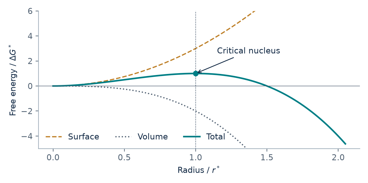
Supersaturation favors the condensed phase through the volume term, while surface energy penalizes small particles. Differentiation gives the critical radius. Smaller clusters tend to shrink; larger ones lower free energy by growing. Growth becomes favorable beyond r* even before the total formation free energy becomes negative. Greater supersaturation lowers both critical size and barrier.
In the isotropic spherical-cap model, a substrate lowers the nucleation barrier through the contact angle. Complete wetting favors spreading. Atomic-scale faceting, strain, and anisotropy modify this model. Deposited atoms compete between diffusion, nucleation, step capture, incorporation, and desorption.
Step flow is favored when diffusion reaches a step before competing events and deposition is sufficiently slow. Lower temperature or higher flux often promotes island nucleation, while heating can also increase desorption. Ostwald ripening transfers material from smaller to larger particles. Thermodynamic equilibrium need not be reached within the available growth time.
3.6 Epitaxy, wetting, and strain
Epitaxy maintains a definite crystallographic relationship between film and substrate. Homoepitaxy uses the same material and heteroepitaxy different materials. Lattice mismatch f=(a_f-a_s)/a_s creates strain. A thin pseudomorphic film follows the substrate in-plane lattice parameter, accumulating elastic energy that can later relax through islands or misfit dislocations.
Frank-van der Merwe growth proceeds layer by layer, typically with favorable wetting and modest strain. Volmer-Weber growth forms 3D islands from the outset, often because of poor wetting. Stranski-Krastanov growth begins with a wetting layer and then islands as strain accumulates; Ge/Si and InAs/GaAs are examples. These morphology classes are distinct from the microscopic step-flow mechanism.
Conduction- and valence-band offsets determine carrier confinement. Type I alignment confines both carriers in one material; type II favors spatial separation; type III has a broken gap. The band gaps alone do not determine the offsets, which also depend on interface dipoles, strain, chemistry, and electron affinities.
3.7 Excitons and optical transitions
A Wannier-Mott exciton is a screened electron-hole bound state. Separate center-of-mass and relative motion; the latter is a hydrogen-like problem with reduced mass μ_r and dielectric constant ε_r. The ground-state binding is R*, placing an excitonic optical line below the quasiparticle gap. Reduced mass and carrier mobility are different quantities despite frequent reuse of the symbol μ.
Using m_e*=0.067m₀, m_h*=0.62m₀, and ε_r=13.2 gives μ_r≈0.0605m₀, a_B≈11.6 nm, and R≈4.72 meV. Room-temperature thermal energy exceeds this binding energy. Optical resonance visibility nevertheless also depends on broadening and kinetics.
The 2D result assumes an ideal 1/r interaction with constant dielectric screening. Real monolayer TMDCs have nonlocal, environment-dependent screening, so neither a universal factor of four nor a fixed 1 eV binding energy applies generally. Direct gaps align conduction and valence extrema in k space; indirect transitions usually require a phonon and have weaker radiative rates.
3.8 Dielectric response and Drude-Lorentz models
With time convention exp(-iωt), a passive medium has κ≥0. The real index describes phase propagation and κ describes attenuation; λ₀ is the vacuum wavelength. Field and intensity 1/e depths differ by a factor of two. Normal-incidence reflectance of a semi-infinite medium differs from the full thin-film problem with multiple interfaces and interference.
The Drude model describes driven, damped free carriers. The low-frequency limit is conductive; weak-collision approximations require ωτ much larger than one. The bare plasma frequency, the screened zero of Re ε, and nanoparticle surface resonances are different quantities. Interband transitions can invalidate a simple Drude model in the visible.
Lorentz oscillators add restoring forces for bound charges and describe resonances such as phonons and bound-electron transitions. Each requires a resonance frequency, oscillator strength, and damping. Absorption and dispersion are linked by causality, while infrared, visible, and ultraviolet spectra can involve different excitations.
4. Probes of nanostructures
4.1 Probe selection and scattering scales
Choose a probe by the quantity required: lattice, composition, morphology, local spectrum, magnetic structure, or transport. Ensemble signals are not automatically representative of one particle. Local probes can correlate properties at the same location but remain sensitive to tips and preparation. Spatial, depth, energy, and temporal resolution are separate metrics.
The electron wavelength formula is nonrelativistic; high-energy TEM requires a relativistic correction. Short wavelength helps resolution, but aberrations, spot size, interaction volume, noise, drift, and specimen stability also matter. Ions transfer momentum efficiently and can sputter atoms. Electrons can cause radiolysis, heating, and knock-on damage.
Elastic electron scattering changes direction with negligible energy loss; inelastic scattering excites phonons, plasmons, or electronic transitions. XPS and AES are surface sensitive mainly because escaping electrons have short inelastic mean free paths, not because the incident radiation is confined to the surface.
4.2 Diffraction and composition spectroscopy
XRD peak positions encode plane spacings and lattice structure; intensities depend on structure factors, texture, and phase fractions. The Scherrer equation estimates coherent-domain size using the peak width in 2θ, in radians. Correct instrumental broadening and consider microstrain. Domain size need not equal particle diameter.
LEED probes surface periodicity and reconstruction through low-energy electron diffraction; larger real-space periods give closer reciprocal-space spots. Grazing-incidence RHEED monitors film growth. SIMS analyzes secondary-ion mass-to-charge ratios for trace composition and depth profiles, but sputter mixing, matrix effects, and material removal complicate interpretation.
XPS measures photoelectron binding energies; for a grounded, uncharged sample, calibration uses the analyzer work function. Core levels identify elements and their chemical environments, but charging can also shift peaks. UPS emphasizes valence states and work function. AES detects electrons emitted during core-hole relaxation, with characteristic energies determined mainly by internal level differences.
UV-Vis measures absorption or extinction; PL, EL, and CL use optical, electrical, and electron-beam excitation. Raman and IR probe vibrations and symmetry. EELS probes local bonding and plasmons, while ellipsometry fits polarization changes to thickness and dielectric response. Matrix elements, selection rules, and modeling prevent these spectra from being universal direct measurements of the full DOS.
4.3 Contrast in SEM, TEM, and STEM
SEM scans a focused beam. Secondary electrons emphasize morphology, backscattered electrons provide composition- and orientation-sensitive contrast, and EDX detects characteristic X-rays. Bright secondary-electron contrast does not uniquely imply high atomic number. Conductive coatings, low voltage, or suitable environmental modes reduce charging in insulators, although coatings alter the surface.
TEM images electrons transmitted through a thin specimen. Bright field selects the direct beam, dark field a diffracted beam, and high-resolution TEM uses interference. Contrast changes with thickness and defocus, so lattice fringes do not identify every atomic species directly. Thinning and focused-ion-beam preparation can introduce damage.
STEM scans a fine probe and detects scattered electrons. HAADF intensity often increases approximately as Z to a power between 1.6 and 2, but thickness, channeling, and collection angles matter. EDX and EELS provide complementary chemical information. Reliable interpretation combines signals rather than assigning composition from brightness alone.
4.4 STM and local tunneling spectroscopy
STM places a conducting tip close to a surface and uses tunneling current for feedback. Constant-current mode records the required height, whereas constant-height mode records current variation. Contrast combines geometry, tip and sample DOS, barrier properties, and bias. Brightness is not necessarily atomic height, and multiple tips, drift, or feedback limitations can create artifacts.
With bias defined on the sample relative to the tip, positive bias mainly probes empty sample states and negative bias occupied states. Differential conductance approximates the LDOS when temperature is low, tip DOS is smooth, transmission varies slowly, and band bending is weak. Normalization by I/V can reduce background but is not universally exact and becomes unstable near zero current.
Estimate apparent barrier height from the slope of ln I, not merely dI/dz. For Φ≈4 eV, increasing separation by 1 Å reduces current by a factor of about 0.129, explaining atomic-scale height sensitivity. Thermal broadening and lock-in modulation also limit spectral resolution.
4.5 AFM, force spectroscopy, and functional probes
AFM senses cantilever deflection or oscillation changes and works on conductors and insulators. Contact mode is affected by friction and adhesion; tapping reduces sustained lateral forces; frequency-modulation noncontact AFM senses force gradients. The displayed frequency-shift expression assumes small amplitude and z as tip-sample separation; large amplitudes require a weighted force average.
A finite tip radius broadens lateral features through tip convolution, so heights are often more reliable than widths. Quantitative force spectroscopy requires spring-constant and deflection-sensitivity calibration. Pull-off force measures adhesion, while approach-retract hysteresis area measures dissipation. Chemical force microscopy uses functional groups for selective interactions.
In KPFM, the force component at the drive frequency is proportional to (V_DC-V_CPD)V_AC. Nulling it determines the contact potential. With V_CPD=(Φ_tip-Φ_sample)/e, a calibrated tip gives sample work function; wiring determines the sign convention. EFM senses electrostatic forces, conductive AFM maps current, and friction microscopy measures torsion.
4.6 Magnetic imaging and near-field optics
MFM detects forces or force gradients from stray fields using a magnetic tip. Lift-mode rescanning suppresses short-range forces, although magnetic signals also weaken with distance. Images are not direct magnetization maps and depend on the tip moment, field derivatives, and domain geometry. The tip can perturb soft magnetic structures. Spin-polarized STM senses spin-dependent tunneling.
SEMPA analyzes secondary-electron polarization for near-surface magnetization. Lorentz TEM detects deflection by transverse magnetic induction: Fresnel imaging emphasizes walls, Foucault imaging selects domains by deflection, and DPC measures vector deflection. Signals integrate induction along the trajectory and can include stray-field or electric contributions; B is not generally equal to μ₀M.
Near-field optics accesses rapidly decaying evanescent fields carrying high spatial frequencies. Aperture NSOM uses a small opening near the specimen, with limited throughput. Scattering-type SNOM uses an illuminated tip to localize and scatter the near field; higher-harmonic demodulation suppresses background. Resolution is governed mainly by the tip and gap, while interpretation depends on dielectric response and geometry.
5. Fabrication of nanostructures
5.1 Lithography, etching, and pattern transfer
A common sequence is cleaning, resist coating, baking, exposure, development, pattern transfer, and resist removal. Positive resist dissolves preferentially where exposed; negative resist retains exposed regions. Etching transfers openings into underlying material. Lift-off deposits material through resist windows and removes the resist with its overlying film. Selectivity, profiles, residue, damage, and overlay all matter.
Optical critical dimension depends on wavelength, numerical aperture, and a process factor k₁. Shorter wavelengths and immersion improve patterning. Resist stochasticity, photon statistics, edge roughness, and overlay also limit features. A technology-node label is not a unique physical linewidth.
Electron-beam lithography writes fine patterns without a mask and is useful for research and mold fabrication. Serial writing limits throughput, while forward and backscattering produce proximity effects. FIB mills, deposits, or prepares cross sections, but implantation and damage must be considered. Particle wavelength alone does not set lithographic resolution.
5.2 Nanoimprint and scanning-probe fabrication
Nanoimprint replicates a hard mold into a polymer using thermal softening or curing. Residual layers must be addressed before subsequent transfer. It provides parallel replication and fine features, with challenges from particles, demolding, residual-layer variation, overlay, and replication of mold defects.
STM and AFM can move adsorbates, transfer atoms with bias pulses, induce local oxidation, or desorb hydrogen passivation. Quantum corrals demonstrate engineered atomic potentials and electron standing waves. Atomic precision comes with limited throughput, stability requirements, and environmental constraints.
5.3 MBE, CVD, ALD, and band engineering
MBE grows crystals using controlled atomic or molecular beams in ultrahigh vacuum. Source temperatures control flux, shutters control sequences, and substrate temperature controls diffusion and desorption. RHEED oscillations can calibrate layer growth when the growth mode supports that interpretation; damping can indicate roughening or a mode change. Purity and precise composition and interfaces are central advantages.
CVD forms solids through precursor reactions at a substrate. MOCVD uses metal-organic sources, often with hydrides, while PECVD activates chemistry through a plasma. Gas transport, surface reactions, and byproduct removal determine growth. Faster deposition does not automatically preserve abrupt interfaces; material chemistry, thermal budget, and uniformity guide method selection.
An ALD cycle alternates precursor A, purge, precursor B, and purge. Self-limiting half-reactions enable thickness control and conformal coating of complex structures. One cycle need not deposit a complete atomic layer. A suitable temperature window, sufficient exposure, and adequate purge are required to avoid nucleation delay, incomplete reactions, or parasitic CVD.
Stacking layers with selected offsets creates wells and superlattices. Separating dopants from the conducting channel reduces ionized-impurity scattering. Gates, contacts, and insulation still require device processing. Growth, band alignment, defects, and fabrication together determine whether quantum effects survive.
5.4 Self-assembly and templating
SK dots exploit strain-driven islanding. Coverage, temperature, mismatch, and diffusion control size and density. Repeated dot and spacer layers can develop vertically correlated positions through elastic fields. Patterned templates can improve positioning and uniformity, but self-assembly does not guarantee identical particles.
Self-assembled monolayers use head-group affinity for a substrate and tail-group chemistry to control the surface. Micelles and reverse micelles form nanoscale reaction environments; reverse-micelle water-core size depends on the water-to-surfactant ratio in a system-specific way. Anodic alumina pores template wire arrays, while steps and reconstructions guide nucleation.
Hydrothermal synthesis uses heated pressurized water for dissolution, reaction, and crystallization and need not be supercritical. Colloidal synthesis often separates rapid nucleation from growth and uses ligands to control stability and facet growth. Phase separation, irradiation, and kinetic instabilities can also create patterns. Equilibrium assembly, kinetic organization, and templated growth are distinct mechanisms.
6. Transport in low-dimensional systems
6.1 The two-dimensional electron gas
A 2DEG forms at a heterojunction or in a MOS inversion layer. Band offsets and electrostatic fields confine carriers normal to the interface while allowing in-plane motion. Modulation doping separates donors from the channel to reduce ionized-impurity scattering. Gates tune density and can laterally define wires and dots.
Here C_g′ is geometric capacitance per area. The first relation neglects traps and quantum capacitance. A finite DOS makes carrier addition shift the chemical potential, producing C_q′. When the DOS is small, geometry alone does not set capacitance. High mobility requires control of impurity, interface, and phonon scattering.
6.2 Landauer conductance and quantum point contacts
Treat the conductor as a scattering region between reservoirs. The one-way 1D DOS times velocity gives an injection rate of 1/h per spin per energy, yielding the Landauer expression after integrating over the bias window. The factor two assumes spin-degenerate channels; explicitly spin-resolved counting uses e²/h.
A QPC opens transverse modes sequentially as gate voltage changes. Nearly unit transmission produces conductance steps of G₀. A perfect spin-degenerate channel still has two-terminal resistance h/(2e²)≈12.91 kΩ, associated with reservoir coupling rather than equivalent local channel dissipation. Reflection, temperature, series resistance, and nonadiabatic geometry modify the plateaus.
6.3 Interference and quantum corrections
The Aharonov-Bohm phase depends on enclosed magnetic flux. Oscillations weaken when paths exceed coherence length or thermal averaging mixes many phases. The Thouless energy corresponds to the inverse diffusion traversal time and provides a scale for thermal averaging and coherent dynamics.
Weak localization arises from enhanced return probability along time-reversed paths and reduces zero-field conductance without strong spin-orbit coupling. A small magnetic field suppresses it. Strong spin-orbit coupling can instead produce weak antilocalization. Coherent samples also show reproducible conductance fluctuations with a characteristic scale set by e²/h, reduced by averaging and geometry.
Ballistic transport describes scattering frequency, coherence describes phase preservation, and localization describes spatial extent. Magnetoresistance interpretation must also consider classical multicarrier response, contacts, and heating.
6.4 Quantum Hall effect and edge states
A perpendicular field quantizes a 2DEG into Landau levels. The filling factor counts density in units of e|B|/h, including occupied spin and valley channels. Unresolved spin often leads to steps of two. Resolved quantization requires cyclotron spacing larger than temperature and broadening; carrier type and field orientation determine the Hall sign.
Disorder localizes some bulk states, permitting a range of density or field over which Hall conductance stays fixed. Boundary confinement produces chiral edge channels. Integer quantization has a topological band interpretation; fractional states require electron interactions and cannot be obtained by independent-particle filling alone.
For n_s=3×10¹¹ cm⁻² and B=5 T, ν≈2.48. This alone does not establish a ν=2 plateau, whose width depends on localization. An observed ν=2 plateau has Hall resistance magnitude about 12.91 kΩ.
6.5 Coulomb blockade and resonant tunneling
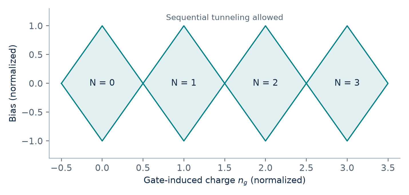
A dot connects to source and drain through tunnel barriers and to a gate capacitively. The constant-interaction model uses total capacitance CΣ. Here E_C=e²/(2CΣ), whereas successive addition chemical potentials differ by 2E_C plus the single-particle spacing. Charging-energy conventions must therefore be stated explicitly.
Sequential tunneling is blocked when no addition chemical potential lies in the bias window. Resolved charge states require sufficiently small thermal and tunnel broadening and weak junction coupling, typically R_t larger than h/e². Gate scans produce Coulomb oscillations; bias-gate maps produce Coulomb diamonds and excited-state lines.
The simple gate period neglects level spacing; generally ΔV_g=(2E_C+Δε)/(eα_g). The resonance formula is for a noninteracting single level, with Γ values in energy units. Its maximum reaches unity for symmetric coupling. Cotunneling can carry residual current inside a blockade region.
7. Graphene, two-dimensional materials, and moiré structures
7.1 Graphene lattice and Dirac dispersion
Graphene has a honeycomb carbon structure with two sublattices on a triangular Bravais lattice. In-plane σ bonds provide structural bonding and p_z orbitals form the low-energy π bands. Inequivalent K and K′ valleys support approximately linear electron and hole dispersions.
The valley index is ξ=±1 and the Pauli matrices act on sublattice pseudospin, not real spin. The velocity is of order 10⁶ m/s. Linear dispersion requires a different DOS from a parabolic band. Ideal neutral graphene has vanishing Dirac-point DOS, while disorder produces electron-hole puddles.
These expressions include two spins and two valleys. Gating crosses from hole to electron doping through neutrality. The lack of a gap supports broadband response but makes a very small off-state current difficult in conventional digital transistors.
7.2 Confinement, magnetic fields, and graphene synthesis
Graphene Landau levels scale as √(|N|B) and include a zero mode. With unresolved fourfold degeneracy, the usual Hall sequence is ±2, ±6, ±10, and so on. Interactions can split the degeneracy. Ideal gapless graphene also permits normal-incidence Klein tunneling through smooth electrostatic barriers, complicating electrostatic confinement.
Nanoribbon boundaries quantize transverse momentum, with gaps influenced by width, armchair or zigzag termination, and edge chemistry. Interlayer coupling changes bilayer dispersion; a perpendicular displacement field can open a tunable gap in AB bilayer graphene. Dimensionality alone does not determine the Hamiltonian.
Mechanical exfoliation yields high-quality flakes, CVD decomposes carbon precursors on catalytic surfaces, and SiC growth enriches surface carbon. Transfer residue, grain boundaries, wrinkles, and contact doping matter. Raman G, 2D, and defect-related D features aid characterization, but shifts can have multiple causes.
7.3 TMDCs, excitons, and valley physics
TMDCs have formula MX₂ and an X-M-X monolayer structure. Semiconducting phases such as MoS₂ and WS₂ can change from indirect bulk gaps to direct monolayer gaps, but not every TMDC or phase is semiconducting. Spin-orbit coupling and broken inversion symmetry couple spin and valley near K and K′.
Time reversal relates opposite valleys and spins. Opposite circular polarizations preferentially excite different valleys under ideal selection rules. Emission polarization P=(I₊-I₋)/(I₊+I₋) diagnoses valley populations, but intervalley scattering, exciton exchange, temperature, and defects govern retention.
Strong excitonic effects separate optical and quasiparticle gaps. Neutral excitons, trions, defect-bound states, and interlayer excitons can produce different lines. Type II bilayers can place electrons and holes in different layers; spacing and twist affect overlap, momentum matching, and lifetime.
7.4 Van der Waals heterostructures and moiré minibands
A twist or lattice mismatch creates slowly varying local stacking and a moiré pattern. The first expression is for identical hexagonal lattices; the second is a small-angle, small-mismatch approximation with θ in radians. For graphene a=0.246 nm and θ=1°, the period is about 14.1 nm.
The parameter α compares interlayer tunneling w with intralayer kinetic energy. Moiré coupling folds bands and can strongly narrow them at suitable parameters. A smaller bandwidth enhances interactions relative to kinetic energy, but a moiré pattern alone does not guarantee flat bands, insulating correlations, or superconductivity. Relaxation, disorder, screening, and filling matter.
The electron count per moiré cell is n_s A_M. A manifold with degeneracy g has full filling density g/A_M. STM, transport, and optics probe local spectra, filling-dependent conduction, and excitonic response respectively.
8. Nanotubes, nanowires, and one-dimensional systems
8.1 Carbon nanotube chirality and band gaps
Rolling graphene along the chiral vector imposes k·C_h=2πq around the circumference. Indices (n,m) determine diameter and chirality: (n,n) is armchair and (n,0) zigzag. Allowed circumferential k lines cut the graphene dispersion into one-dimensional subbands.
In ideal nearest-neighbor zone folding, tubes with n-m divisible by three are metallic and the others semiconducting, with gaps approximately inversely proportional to diameter. Curvature and strain can open small gaps in nominally metallic non-armchair tubes. Excitonic effects also separate optical transitions from single-particle gaps.
A (10,0) tube has diameter about 0.783 nm and is semiconducting; a (10,10) tube is about 1.36 nm and armchair metallic. With γ₀=2.7 eV and a_CC=0.142 nm, the first tube has a simple-model gap near 0.98 eV, subject to small-diameter corrections.
8.2 Nanotube synthesis, transport, and spectroscopy
Arc discharge, laser ablation, and catalytic CVD produce nanotubes. In CVD, metal nanoparticles assist precursor decomposition and growth. Catalyst size influences diameter but does not uniquely select chirality. Single-wall and multiwall tubes differ in channels, coupling, defects, and contact behavior.
An ideal metallic single-wall tube has two orbital channels and two spins, giving 4e²/h and about 6.45 kΩ at perfect transmission. Contacts, defects, and barriers often dominate and can create Coulomb-blockaded dots. Strong one-dimensional interactions can invalidate a simple independent-quasiparticle Drude picture.
The Raman radial-breathing frequency generally rises as diameter decreases. G-band features and resonance conditions add structural information. STS van Hove peaks, polarized absorption, and emission provide complementary constraints, with environmental, strain, and excitonic effects affecting assignments.
8.3 Semiconductor nanowires and VLS growth
VLS growth supplies vapor precursors, dissolves growth species into a liquid catalyst, and precipitates crystal at a supersaturated liquid-solid interface. The droplet collects material and defines the growth front. Diameter also depends on wetting, temperature, flux, and sidewall deposition. VSS uses a solid catalyst, and catalyst-free routes also exist.
Precursor switching forms axial heterostructures, while sidewall deposition creates radial core-shell structures. Axial barriers define dots; shells enable passivation, separation, or conducting channels. Surface depletion can span a thin wire, making surface states and gate dielectrics central to threshold, mobility, and noise.
Nanowires support FETs, detectors, emitters, and sensors, with performance governed by contacts, trapping, doping, and heat flow. Length, diameter, phase, defects, and surface condition all matter; one-dimensional geometry alone does not fix device performance.
9. Nano-optoelectronics and plasmonics
9.1 Quantum-well transitions, superlattices, and lasers
Interband transitions combine the gap, electron and hole confinement, and exciton binding. Their strength depends on Bloch matrix elements, envelope overlap, and polarization. Matching envelope quantum numbers often overlap strongly in ideal similar symmetric wells, while asymmetry and fields change the selection rules.
Intersubband transitions stay within one band. Ideal conduction-band well transitions require an electric-field component normal to the layers. Symmetric-well dipole transitions connect opposite parities. Normal-incidence plane waves lack that field component, motivating waveguide or grating coupling. Quantum cascade lasers use engineered intersubband electron transitions.
Coupled periodic wells form minibands and minigaps. A perpendicular field tilts levels and can reduce delocalization. The quantum-confined Stark effect often redshifts transitions while reducing electron-hole overlap. Lasing additionally requires inversion and gain exceeding cavity loss; enhanced DOS alone is insufficient.
9.2 Quantum-dot spectra and emission efficiency
A Brus-type spherical effective-mass model adds electron and hole confinement and a Coulomb attraction to the bulk gap. Confinement scales as R⁻² and attraction as R⁻¹, usually producing a blue shift as strongly confined dots shrink. Finite barriers, dielectric mismatch, atomistic structure, and surface states limit quantitative accuracy.
For R much smaller than the exciton radius, electron and hole confinement is strong; for much larger R, exciton center-of-mass confinement is a useful picture. Size distributions cause inhomogeneous broadening, while phonons and lifetime produce homogeneous broadening. Core-shell passivation can suppress nonradiative loss but also changes strain and offsets.
Interpret yield and lifetime together: a long lifetime can reflect slow radiative recombination or trapping. Yield 0.8 and lifetime 20 ns imply radiative and nonradiative rates of 4×10⁷ and 1×10⁷ s⁻¹. Charging, traps, and Auger processes cause blinking or multiexciton quenching; narrow emission does not ensure high yield.
9.3 Localized surface plasmons
LSPR is a collective oscillation of conduction electrons against the ionic background. The dipole polarizability above applies to a small sphere in a uniform dielectric in the quasistatic limit. A small real denominator favors resonance, while losses limit amplitude. Polarizability α_p is distinct from absorption coefficient α.
The size scalings apply in the small-particle dipole limit. Absorption dominates smaller particles, with scattering relatively stronger as size grows. Retardation, radiative damping, and multipoles eventually matter. Nanorods have direction-dependent depolarization, and increasing environmental index commonly redshifts resonances.
Gaps concentrate optical fields and can enhance Raman signals and transitions. At subnanometer separation, nonlocal response and tunneling limit classical field-enhancement predictions. Extinction includes both absorption and scattering, so it does not directly measure heat deposition.
9.4 Propagating surface modes and near-field applications
SPPs propagate along a metal-dielectric interface and decay away from it. Bound modes require sufficiently negative metal permittivity in the low-loss picture. Their in-plane momentum usually exceeds that of free-space light, requiring prism, grating, or near-field coupling. The propagation length shown is an intensity 1/e length.
For an ideal Drude metal in vacuum, the high-wavevector planar SPP asymptote is ω_p/√2, the spherical LSPR is ω_p/√3, and the bulk plasma frequency is ω_p. Different boundary conditions produce these values. Strong confinement often increases loss, creating tradeoffs among enhancement, propagation, bandwidth, and heating.
A metal environment can enhance radiative mode density or increase nonradiative energy transfer. Field enhancement, faster total decay, and brighter far-field emission are therefore different observations and require joint interpretation of yield, lifetime, and collection efficiency.
10. Magnetic nanostructures and spintronics
10.1 Exchange, anisotropy, and single domains
Magnetism combines exchange, spin-orbit coupling, and dipolar interactions. With the displayed convention, positive J favors parallel spins. Ferromagnets have spontaneous net magnetization, antiferromagnetic sublattices can cancel, and ferrimagnets have unequal opposing moments. Crystal, shape, surface, and interface anisotropies determine easy directions.
Domains reduce stray-field energy but cost wall energy. A sufficiently small particle favors a single domain; smaller still, thermal reversal becomes important. Single-domain structure does not ensure stable magnetization. Reduced coordination can alter local moments, while oxidation and surface spin disorder can reduce net magnetization.
Here A is exchange stiffness and K anisotropy energy density in a simple continuum wall model. Exchange smooths magnetization and stronger anisotropy narrows walls. Shape and interfaces tune coercivity, while real reversal can involve nucleation, wall motion, or nonuniform rotation.
10.2 Superparamagnetism and thermal stability
A uniaxial single-domain particle has opposing easy-axis states separated by an approximate K_eff V barrier. Néel activation reverses its moment. If the observation time greatly exceeds the reversal time, zero-field averaging gives superparamagnetic behavior; if reversal is much slower, the particle is blocked. Blocking temperature depends on measurement time.
Superparamagnetism retains internal magnetic order while the total moment fluctuates. Above the Curie temperature, internal long-range order is lost instead. In liquids, whole-particle Brownian rotation adds relaxation. Interparticle coupling, size distributions, and surface anisotropy can invalidate a single-barrier model.
For K_eff=10⁵ J/m³, T=300 K, τ₀=10⁻⁹ s, and t_m=100 s, the required barrier ratio is about 25.3, giving V≈1.05×10⁻²⁴ m³ or spherical diameter about 12.6 nm. This is a parameter-specific estimate, not a universal superparamagnetic size.
10.3 Magnetic composites and interface coupling
Hard magnetic phases resist reversal through strong anisotropy; soft phases rotate more easily and can supply large magnetization. Exchange-coupled composites can combine these properties only with suitable soft-phase dimensions and interface coupling. A nonmagnetic matrix also controls spacing, oxidation, and dipolar interactions.
Ferromagnet-antiferromagnet interfaces can produce exchange bias, shifting hysteresis loops and stabilizing reference layers. Interlayer coupling can depend on spacer thickness and favor parallel or antiparallel alignment. Saturation, remanence, coercivity, loop shape, and temperature dependence provide complementary information.
10.4 GMR, TMR, and spin transport
Spintronics uses charge and spin. GMR stacks separate ferromagnetic metals with a nonmagnetic metal spacer. Spin-dependent scattering usually gives lower resistance for parallel alignment. In the two-current picture, one spin channel stays weakly scattered in the parallel state, while both encounter a strongly scattering layer in the antiparallel state. Spin diffusion length differs from phase coherence length.
A magnetic tunnel junction replaces the metal spacer with an insulator. The Jullière expression assumes spin-conserving tunneling and simplified DOS weighting; crystalline barrier symmetry can alter it. Equal polarizations of 0.4 give about 38.1% TMR in this model. GMR and TMR involve different transport mechanisms.
Spin injection depends on interface properties and resistance matching. Transferred spin angular momentum can exert torque and switch magnetization. Memory design balances writing, readout, and thermal stability. Angular, temperature, and hysteresis measurements distinguish spin-valve response from anisotropic or ordinary orbital magnetoresistance.
11. Worked derivations and calculations
11.1 Finite-well counting and Airy states
For m=m₀, L=1 nm, and V₀=1 eV, use the infinite-well energy 0.376 eV to obtain X=√(1/0.376)≈1.63, hence two bound states. Solve the even and odd matching equations for 0<z<z₀, then recover E=-V₀+2ℏ²z²/(mL²).
For V(x)=Fx with positive energy slope F, introduce ℓ=(ℏ²/2mF)^(1/3), ε₀=Fℓ, and ξ=x/ℓ-E/ε₀. The Schrödinger equation becomes the Airy equation. Ai decays at positive infinity while Bi diverges, so bound solutions retain only Ai.
For a triangular half-well with a hard wall at x=0, Ai(-E/ε₀)=0. If a_n denotes its nth negative zero, E_n=|a_n|ε₀, with the first coefficients 2.3381, 4.0879, and 5.5206. These are exact Airy-zero eigenvalues.
For V=F|x|, extend the positive-half-line solution by parity. Even states obey Ai′(-E/ε₀)=0 and odd states Ai(-E/ε₀)=0. The ground state is even at 1.01879ε₀, followed by 2.33811ε₀ and 3.24820ε₀.
The WKB expression follows from action quantization between two turning points. It is a large-quantum-number approximation for the symmetric V potential, not the exact spectrum. The half-well has a different boundary phase.
11.2 A spherical dot and its shells
For an infinite spherical well, separation gives spherical harmonics and regular spherical Bessel functions. The wall sets their zeros. The ground state uses the first zero π of j₀(x)=sin x/x. R is the radius; using diameter in its place introduces a factor-of-four energy error.
The first zeros π, 4.4934, 5.7635, and 2π label 1s, 1p, 1d, and 2s shells. Neglecting spin-orbit coupling, shell capacities are 2(2l+1), including spin. Cumulative closures are 2, 8, 18, and 20 for this hard-wall model, not universal cluster magic numbers.
11.3 Confinement and dimensional filling scales
The free-electron confinement energy is 0.3760/L(nm)² eV. Widths 1 Å, 1 nm, 100 nm, and 1 μm give 37.60 eV, 0.3760 eV, 3.760×10⁻⁵ eV, and 3.760×10⁻⁷ eV. Multiply by m₀/m* for other masses. The last two are much smaller than room-temperature thermal energy.
Compare donor fraction x=10⁻⁴ with common lattice spacing a, complete ionization, one valley, and spin degeneracy two. Densities are n₃=x/a³, n₂=x/a², and n₁=x/a; they have different units. In units E_a=ℏ²/(2ma²), the Fermi energies are:
Enhanced concentration of states near lower-dimensional band edges reduces the filling energy for dilute carriers in this comparison. Real low-temperature semiconductors can exhibit dopant freeze-out, requiring ionization balance as well as carrier counting.
11.4 Magnetic energy and 2D transport examples
At m*=0.1m₀ and B=5 T, the cyclotron spacing is 5.79 meV. For an InSb model with m*=0.014m₀ and |g*|=51 at 5 T, it is 41.35 meV, compared with Zeeman splitting 14.76 meV. The shifts are ±half the splitting.
For a 2D Hall bar with I=1 μA, B=1 T, |V_H|=2 mV, V_L=1 mV, and l/w=2, obtain n_s=3.12×10¹⁵ m⁻², R□=500 Ω, and μ=4.00 m²/(V·s)=4.00×10⁴ cm²/(V·s). Nonlinear Hall data would require reassessing the model.
For CΣ=20 aF, C_g=2 aF, and negligible level spacing, E_C=4.01 meV, addition energy≈8.01 meV, gate lever arm 0.1, and gate period≈80.1 mV. At 4 K, thermal energy is about 0.345 meV, but clear blockade also requires sufficiently weak tunnel coupling.
11.5 Plasma-frequency and dielectric calculations
For FCC Au with a=4.08 Å and one free electron per atom, n=4/a³≈5.89×10²⁸ m⁻³ and ℏω_p≈9.01 eV. A diamond Si cell has eight atoms and 32 valence electrons; at a=5.43 Å this gives n_v≈2.00×10²⁹ m⁻³ and a valence-plasmon scale near 16.6 eV. This is not the free conducting carrier density of silicon.
Use E=ℏω=hf, E_p=ℏω_p, and E_γ=ℏγ consistently in eV. The following exact-model values assume ε∞=1, E_p=3.8 eV, and E_γ=0.02 eV; they are not measured constants for a real metal over the full spectrum. RF and microwave frequencies require the full Drude expression.
| Spectral range | ωτ | n | κ | Field skin depth / nm |
|---|---|---|---|---|
| RF: 10 MHz | 2.068e-06 | 9.343e+04 | 9.343e+04 | 5.107e+04 |
| Microwave: 2.45 GHz | 0.0005066 | 5967 | 5970 | 3262 |
| IR: 2 μm | 31 | 0.1002 | 6.045 | 52.65 |
| Visible: 550 nm | 112.7 | 0.009288 | 1.357 | 64.51 |
| DUV: 200 nm | 310 | 0.7901 | 0.0007671 | 4.149e+04 |
Compute the field skin depth from δ_E=λ/(2πκ), then divide by two for intensity depth. At λ=2 μm, n≈0.1002 rather than 0.01; substitution into ε₂=2nκ checks the result. Dimensional analysis, limits, and back-substitution provide useful cross-checks.
11.6 Beam recoil, diffraction size, and dipole forces
For 5 keV probes striking a stationary Si atom of mass about 28u, maximum elastic recoil is about 0.39 eV for electrons, 4.84 keV for 40u Ar ions, and 1.9×10⁻³ eV for backscattered photons. These are head-on elastic limits, not total damage rates; inelastic electron and photon processes also cause damage.
For λ=0.154 nm, 2θ=40°, and corrected β=0.40°, convert β to 0.006981 rad and use θ=20°. The Scherrer estimate is about 21.1 nm. Confusing θ with 2θ or degrees with radians gives erroneous sizes.
The force formulas assume equal parallel dipoles aligned with their separation in vacuum, giving attraction. At p=10⁻²⁹ C·m and r=1 nm, the electric force is about 5.39 pN; for magnetic moments of 1μ_B it is about 5.16×10⁻¹⁷ N. Other orientations change magnitude and sign.
11.7 Connecting observables to physical models
If smaller dots show a blue-shifted absorption edge, compare radius with exciton size and test confinement scaling. Then assess composition, strain, and oxidation. Combine TEM size distributions with absorption and single-particle PL; one ensemble spectrum cannot uniquely recover every particle size.
For low-temperature conductance steps, examine series resistance, transmission, and spin or valley degeneracy. Check temperature and gate dependence. Periodic Coulomb peaks and diamonds indicate islands and tunnel barriers rather than a simple smooth QPC.
If coercivity vanishes on warming, compare measurement time with Néel reversal time and test frequency dependence. Loss of hysteresis alone does not establish a Curie transition; evidence on internal magnetic order is also needed.
A consistent method is to specify geometry and boundaries, compare scales, choose a valid model, define conventions, compute observables, and check units, limits, and artifacts. An observed feature constrains a model rather than replacing its derivation.
11.8 Writing time, dopant potentials, and reverse micelles
For parallel 10 nm by 10 nm trenches at 50 nm pitch across 1 cm by 1 cm of silicon, total line length is area divided by pitch, or 2000 m. Removed volume is 2×10⁻¹³ m³, containing about 10¹⁶ atoms at silicon density 5.0×10²⁸ m⁻³.
For singly charged ions at 1 μA and sputter yield one, ideal writing time is about 26.7 minutes. This neglects overhead, incomplete beam utilization, redeposition, and angle-dependent yield. Serial writing time scales with the total removed material.
A uniformly ionized donor slab has positive charge density en_d. Poisson’s equation and central symmetry give a parabolic electron potential within the slab, with spring constant k=e²n_d/(ε₀ε_r) and frequency √(k/m*). The parabola applies inside the doped region; real screening requires a self-consistent Schrödinger-Poisson solution.
For a spherical reverse-micelle water core, let v_w be molecular water volume and a_s surfactant head-group area. Volume and surface counting give diameter proportional to the water-to-surfactant molar ratio, with length coefficient 6v_w/a_s. The model assumes all water lies in the core, all surfactant coats it, and limited polydispersity; tail thickness and free species modify it.
12. Self-assessment, formula use, and terminology
12.1 Self-assessment questions
-
Is every 20 nm film a single-subband 2DEG? 2. How does the ground energy change if well width doubles and mass halves? 3. Does constant 2D DOS imply uniform electron occupation in energy? 4. Can a system be both diffusive and coherent?
-
Does XRD broadening uniquely imply smaller particles? 6. Why can STM apparent height change with bias? 7. How do layer, island, and SK growth differ, and where does step flow fit? 8. Why does a perfect 1D channel have finite two-terminal resistance?
-
Where do e²/(2CΣ) and e²/CΣ appear in a dot? 10. Is a ν=2 Hall plateau the same experiment as two spin-degenerate QPC modes? 11. How do graphene and parabolic 2D DOS differ? 12. Does a moiré pattern guarantee superconductivity?
-
Classify (12,0) and (13,0) tubes by zone folding. 14. Why do well intersubband transitions require specific polarization? 15. How do LSPR and SPP differ spatially? 16. Does zero time-averaged moment imply no internal magnetic order?
12.2 Answers and reasoning
-
No; compare subband spacing, Fermi energy, and temperature. 2. One half, since E∝1/(mL²). 3. No; occupied density is D(E)f(E). 4. Yes, when ℓ≪L≪Lφ.
-
No; microstrain and instrument response also broaden peaks. 6. STM height mixes geometry with energy-dependent LDOS. 7. Layer growth spreads, island growth starts in 3D, and SK changes from wetting layer to islands; step flow describes incorporation at steps. 8. Reservoir mode injection yields a quantum contact contribution without requiring ideal-channel dissipation.
-
The former defines E_C here; the latter is the electrostatic addition-energy contribution. 10. No; one measures transverse Hall resistance and the other longitudinal QPC conductance, with two spin-degenerate QPC modes giving 4e²/h. 11. Graphene DOS is proportional to |E|; a parabolic 2D subband has constant DOS. 12. No; band structure, filling, interactions, and quality matter.
-
(12,0) is nominally metallic, possibly with a curvature gap; (13,0) is semiconducting. 14. The transition dipole lies along the confinement direction. 15. LSPR is particle-localized; SPP propagates along an interface and decays normally. 16. No; an internally ordered superparamagnetic particle can thermally reverse its net moment.
12.3 Constants, units, and conventions
Conversions: 1 eV=1.602176634×10⁻¹⁹ J; 1 Å=0.1 nm; 1 cm⁻²=10⁴ m⁻²; 1 cm⁻³=10⁶ m⁻³; 1 cm²/(V·s)=10⁻⁴ m²/(V·s); 1 aF=10⁻¹⁸ F. Ordinary frequency f and angular frequency ω=2πf give energies hf and ℏω respectively.
Use e>0 and electron charge -e. The vacuum mass is m₀ and band mass m*. Reduced exciton mass is μ_r, mobility μ_e/h, and chemical potential μ when specified. E_C denotes charging energy and E_c a conduction-band edge. Tunneling κ is an inverse length, whereas optical κ is dimensionless.
State DOS normalization, energy reference, and degeneracies. Distinguish conductance, conductivity, resistance, resistivity, and sheet resistance. Distinguish quasiparticle gap from optical excitation and field decay from intensity decay. In magnetism B=μ₀(H+M), rather than universally μ₀M.
12.4 Key terms and physical connections
Quantum confinement, subbands, DOS, Fermi energy, tunneling, coherence, dephasing, mean free path, effective mass, excitons, and localization connect boundary conditions to spectra, occupation, and transport or optical response.
Surface reconstruction, relaxation, nucleation, epitaxy, wetting, step flow, self-assembly, and passivation connect surface free energies and competing rates to morphology, defects, and material properties.
Quantum point contacts, Coulomb blockade, Landau levels, valleys, pseudospin, moiré minibands, plasmons, superparamagnetism, and spin valves illustrate how scales, degeneracy, interactions, and boundaries create nanoscale device behavior.